- 您现在的位置:买卖IC网 > Sheet目录1994 > DS17285S-3NT (Maxim Integrated Products)IC RTC 3V 2K NV RAM 24-SOIC
DS17285/DS17287/DS17485/DS17487/DS17885/DS17887
Real-Time Clocks
_____________________________________________________________________
7
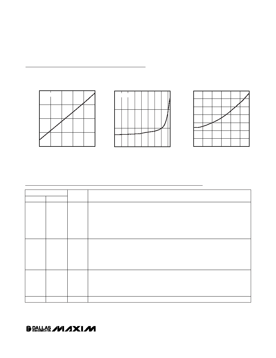
SUPPLY CURRENT
vs. INPUT VOLTAGE
DS17285/87
toc01
VBAT (V)
SUPPLY
CURRENT
(nA)
3.5
3.3
3.0
2.8
250
300
350
400
200
2.5
3.8
VCC = 0V
SUPPLY CURRENT
vs. TEMPERATURE
DS17285/87
toc02
TEMPERATURE (
°C)
SUPPLY
CURRENT
(nA)
65
50
35
20
5
-10
-25
300
350
400
250
-40
80
VBAT = 3.0V
OSCILLATOR FREQUENCY
vs. SUPPLY VOLTAGE
DS17285/87
toc03
SUPPLY VOLTAGE (V)
OSCILLATOR
FREQUENCY
(Hz)
5.0
4.5
4.0
3.5
3.0
32768.1
32768.2
32768.3
32768.4
32768.5
32768.6
32768.7
32768.0
2.5
5.5
Typical Operating Characteristics
(VCC = +3.3V, TA = +25°C, unless otherwise noted.)
Pin Description
PIN
24
28
NAME
FUNCTION
1
8
PWR
Active-Low Power-On Reset. This open-drain output pin is intended for use as an on/off
control for the system power. With VCC voltage removed from the device,
PWR can be
automatically activated from a kickstart input by the
KS pin or from a wake-up interrupt.
Once the system is powered on, the state of
PWR can be controlled by bits in the control
registers. The
PWR pin can be connected through a pullup resistor to a positive supply. For
5V operation, the voltage of the pullup supply should be no greater than 5.7V. For 3V
operation, the voltage on the pullup supply should be no greater than 3.9V.
2, 3
9, 10
X1, X2
Connections for Standard 32.768kHz Quartz Crystal. The internal oscillator circuitry is
designed for operation with a crystal having a specified load capacitance (CL) of 6pF or
12.5pF. Pin X1 is the input to the oscillator and can optionally be connected to an external
32.768kHz oscillator. The output of the internal oscillator, pin X2, is left unconnected if an
external oscillator is connected to pin X1. These pins are missing (N.C.) on the EDIP
package.
4–11
12–17,
19, 20
AD0–AD7
Multiplexed Bidirectional Address/Data Bus. The addresses are presented during the first
portion of the bus cycle and latched into the device by the falling edge of ALE. Write data is
latched by the rising edge of
WR. In a read cycle, the device outputs data during the latter
portion of the
RD low. The read cycle is terminated and the bus returns to a high-impedance
state as
RD transitions high.
12, 16
21, 22, 26
GND
Ground
发布紧急采购,3分钟左右您将得到回复。
相关PDF资料
DS1742-100IND
IC RTC RAM Y2K 5V 100NS 24-EDIP
DS1743P-70+
IC RTC RAM Y2K 5V 70NS 34-PCM
DS1744-70IND
IC RTC RAM Y2K 5V 70NS 28-EDIP
DS1746-70IND
IC RTC RAM Y2K 5V 70NS 32-EDIP
DS1747W-120IND
IC RTC RAM Y2K 3.3V 120NS 32EDIP
DS17887-3-IND
IC RTC 3V 8K NV RAM 24-EDIP
DS1851E-010+
IC DAC DUAL NV TEMP CNTRL 8TSSOP
DS2187S+
IC RECEIVE LINE INTERFACE 20SOIC
相关代理商/技术参数
DS17285S-5
制造商:Rochester Electronics LLC 功能描述: 制造商:Maxim Integrated Products 功能描述:
DS17285S-5/T&R
制造商:Maxim Integrated Products 功能描述:IC RTC 5V 2K NV RAM 24-SOIC
DS17285S-5/T&R
功能描述:实时时钟 RoHS:否 制造商:Microchip Technology 功能:Clock, Calendar. Alarm RTC 总线接口:I2C 日期格式:DW:DM:M:Y 时间格式:HH:MM:SS RTC 存储容量:64 B 电源电压-最大:5.5 V 电源电压-最小:1.8 V 最大工作温度:+ 85 C 最小工作温度: 安装风格:Through Hole 封装 / 箱体:PDIP-8 封装:Tube
DS17285S-5+
功能描述:实时时钟 3V/5V RTC K Multiplexed Kick-S RoHS:否 制造商:Microchip Technology 功能:Clock, Calendar. Alarm RTC 总线接口:I2C 日期格式:DW:DM:M:Y 时间格式:HH:MM:SS RTC 存储容量:64 B 电源电压-最大:5.5 V 电源电压-最小:1.8 V 最大工作温度:+ 85 C 最小工作温度: 安装风格:Through Hole 封装 / 箱体:PDIP-8 封装:Tube
DS17285S-5+T&R
制造商:Maxim Integrated Products 功能描述:REAL TIME CLOCK MULTIPLEXED 2KBYTE 24SOIC - Tape and Reel 制造商:Maxim Integrated Products 功能描述:Maxim Integrated DS17285S-5+T&R Real Time Clocks (RTC) 制造商:Maxim Integrated Products 功能描述:IC RTC 5V 2K NV RAM 24-SOIC
DS17285S-5+T&R
功能描述:实时时钟 3V/5V RTC K Multiplexed Kick-S RoHS:否 制造商:Microchip Technology 功能:Clock, Calendar. Alarm RTC 总线接口:I2C 日期格式:DW:DM:M:Y 时间格式:HH:MM:SS RTC 存储容量:64 B 电源电压-最大:5.5 V 电源电压-最小:1.8 V 最大工作温度:+ 85 C 最小工作温度: 安装风格:Through Hole 封装 / 箱体:PDIP-8 封装:Tube
DS17285SN-
制造商:MAXIM 制造商全称:Maxim Integrated Products 功能描述:Real-Time Clocks
DS17285SN3
制造商:MAXIM 制造商全称:Maxim Integrated Products 功能描述:Real-Time Clocks